Dilip Rana
Who is Dilip Rana?
I am Dilip Rana. I am currently a PhD Researcher focusing on Power Electronics, specificically working on the reliability characterization of GaN power devices at cryogenic temperatures.
Personal website of Dilip Rana
Please find my personal website here: diliprana.github.io
What are focus areas of Dilip?
It includes, Power Electronics, Reliability Assessment of Power Devices, specifically GaN (Gallium Nitride) HEMTs (High Electron Mobility Transistors). I have been focusing on the operation of these at cryogenic temperatures (extremly cold environment, currently as low as 50 K).
Where is Dilip Rana from?
I am from Kathmandu, Bagmati Nepal. I am currently living in Troy, New York and pursuing my PhD at RPI (Rensselaer Polytechnic Institute).
What is the educational qualification of Dilip Rana?
With bachelor's degree in electrical engineering I got in 2022, I am a direct PhD student now at RPI in Electrical and Electronics Engineering.

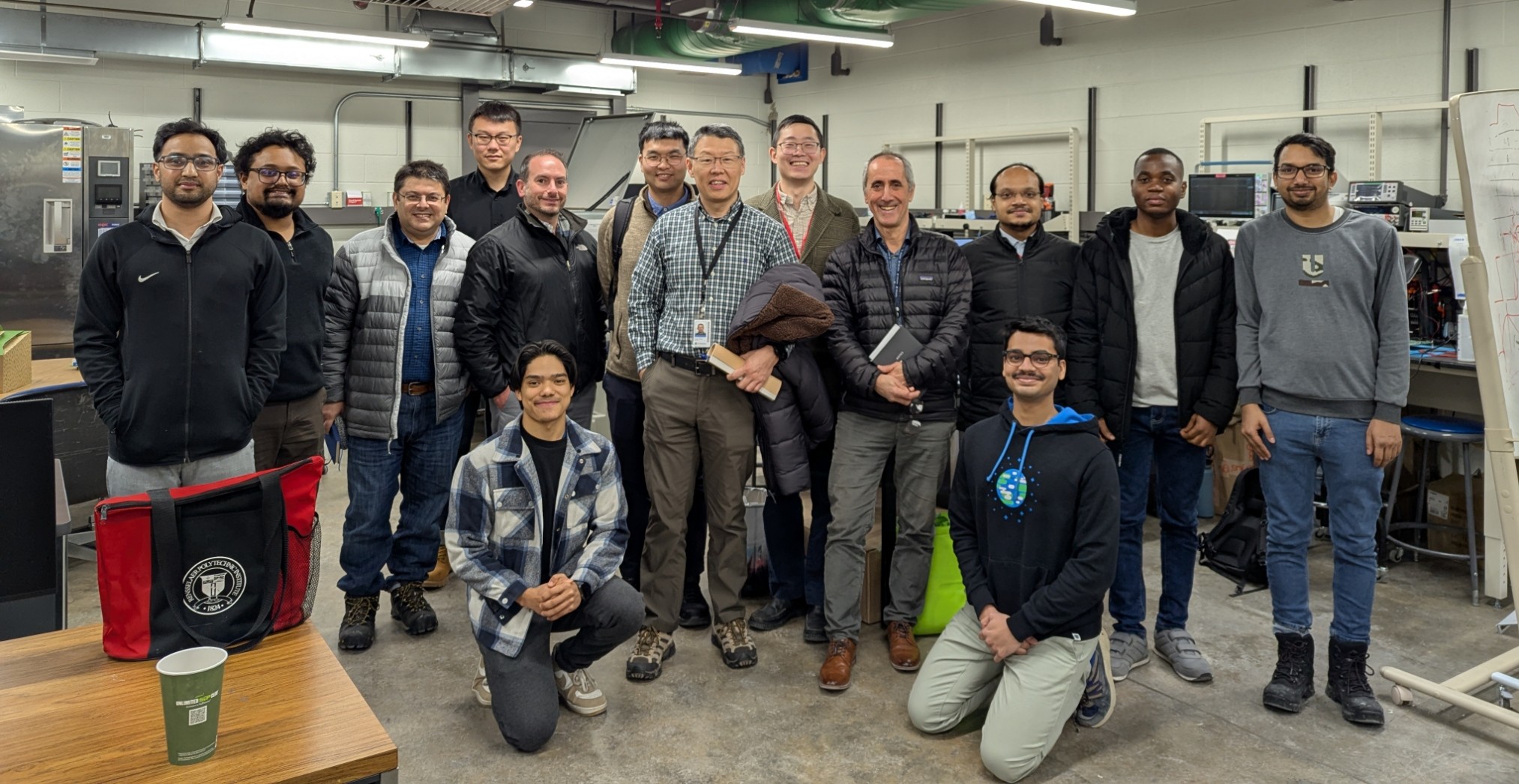
I am currently a graduate research assistant working with Prof. Zheyu Zhang. Currently, I am honored to be involved in a NASA-funded project focused on evaluating the suitability of GaN HEMTs for future lunar missions. My work involves conducting stress tests that replicate lunar environmental conditions and assessing device performance to support the design of next-generation power converters. My research centers on the reliability assessment of GaN HEMTs, with a strong focus on understanding their behavior under extreme operating conditions.

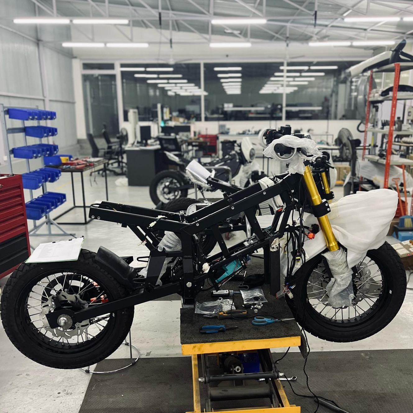
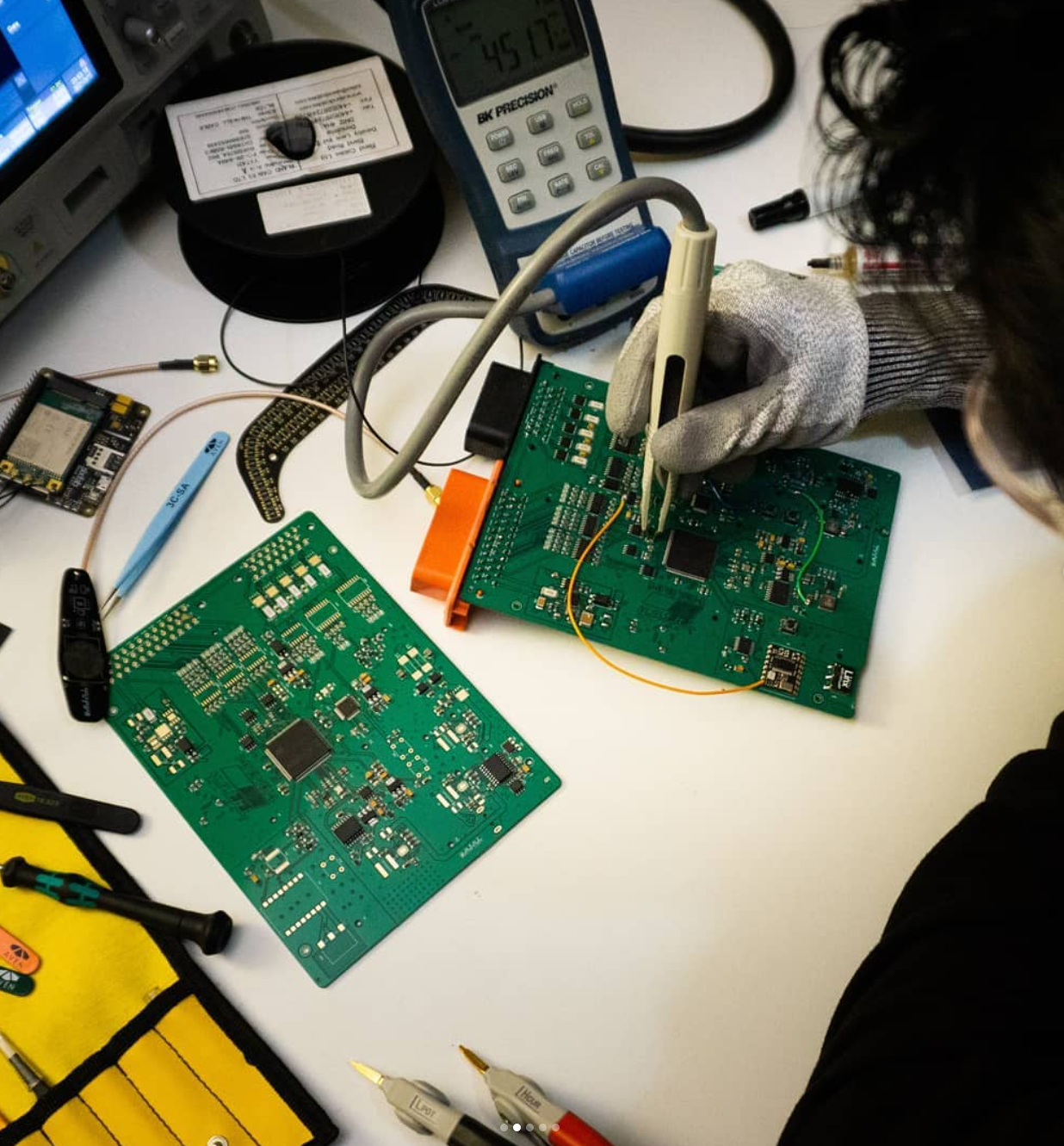
Following a three-month internship, I joined Yatri Motorcycles—Nepal’s first and only electric two-wheeler startup—as a full-time Embedded Hardware Engineer. I was involved in the design, testing, and implementation of critical hardware components for vehicle embedded systems, including the Vehicle Control Unit (VCU), power relay boards, and more. This role required close collaboration with multidisciplinary teams for system-level testing and design validation. Seeing these developments successfully integrated into the final product was a highly rewarding experience.
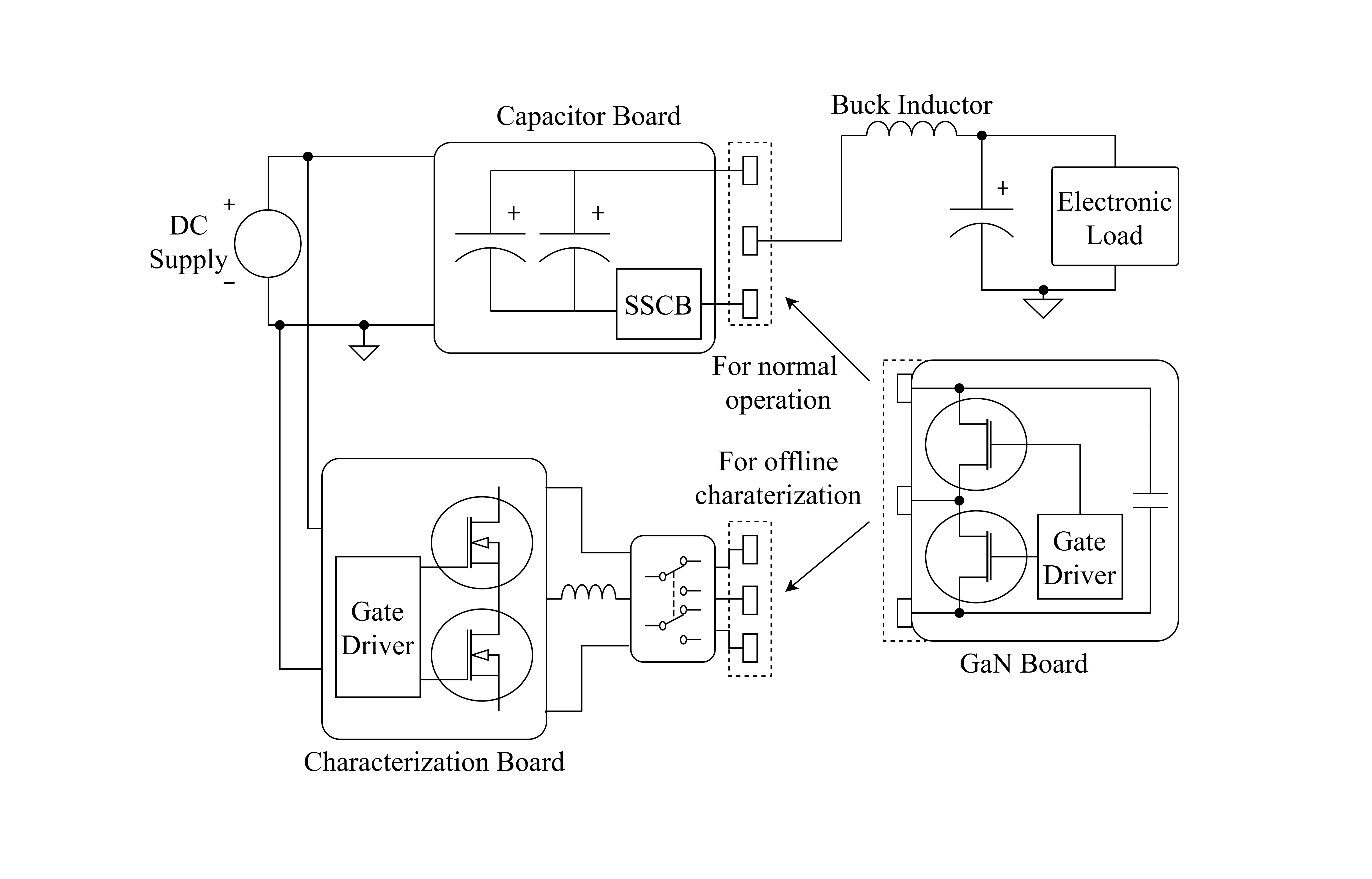
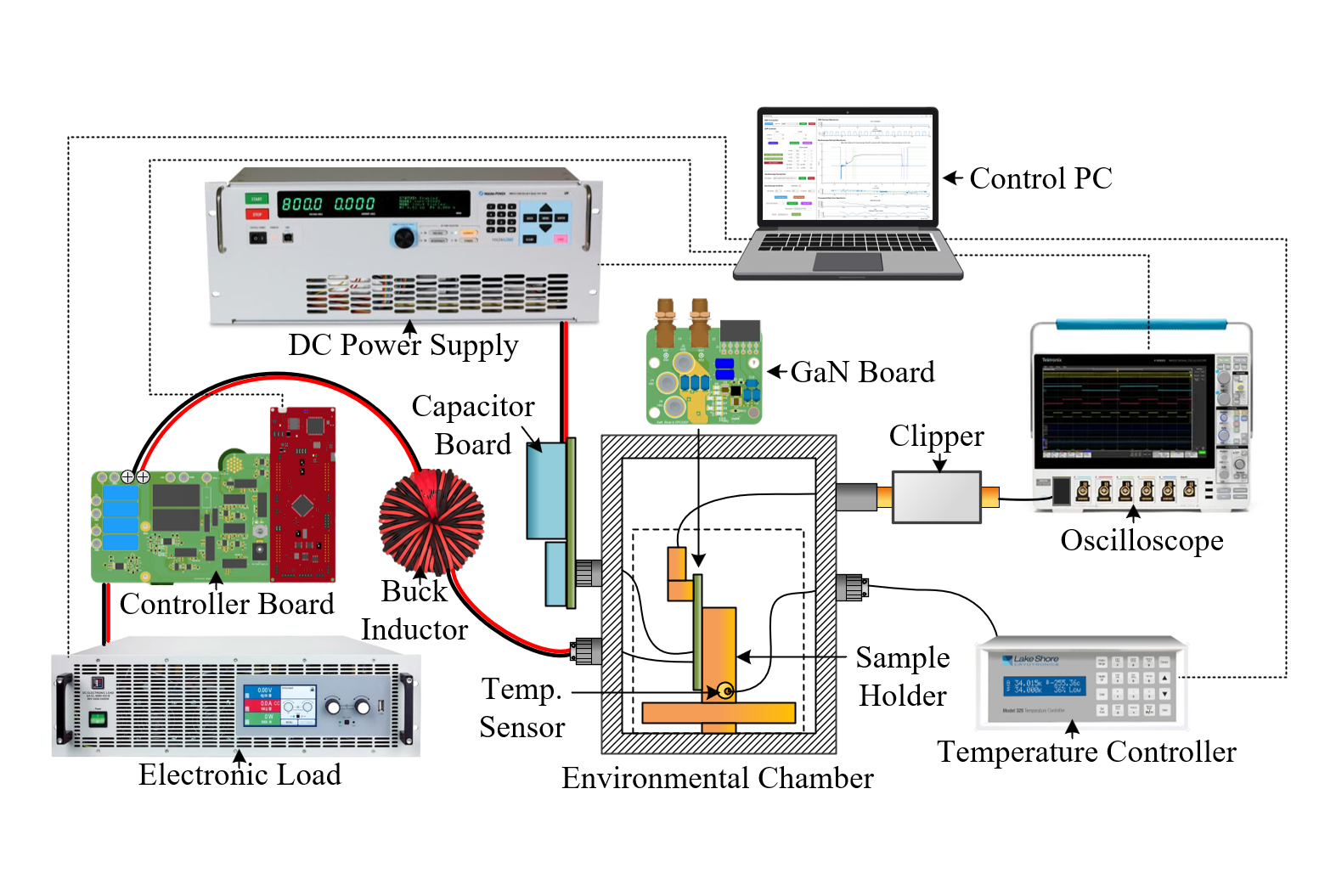
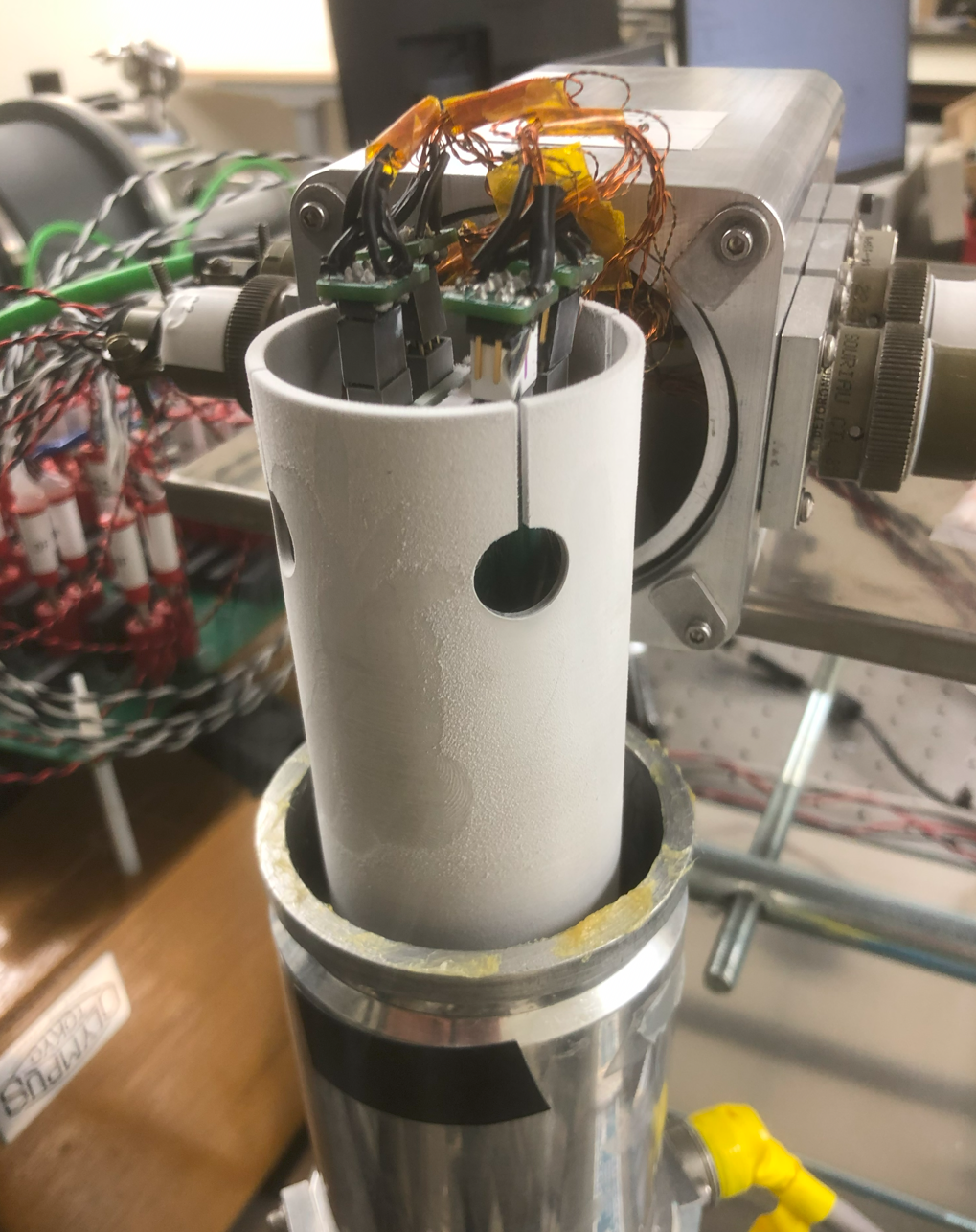
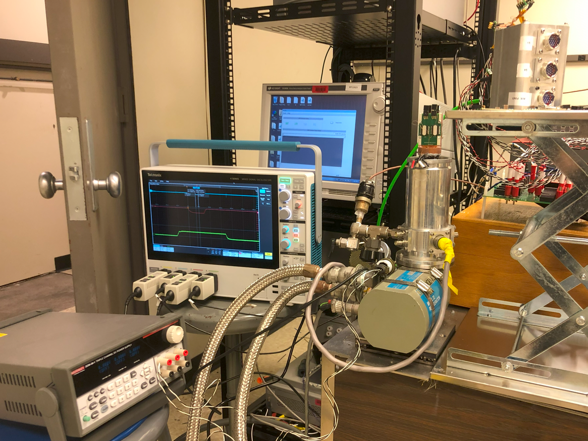
To understand the degradation of GaN HEMTs under actual power converter operating conditions across a wide range of environments, reliability tests are performed on commercial GaN HEMTs.
How:
- An environmental chamber using liquid helium based cryocooler and heater to achieve required temperature range
- Design of realistic stress emulation platform with online monitoring
- Periodic offline characterization for I-V characteristics extraction
Since prior studies showed promising GaN HEMT performance beyond manufacturer-specified temperature limits, we conducted static characterization across these extreme ranges. This allowed us to examine temperature-dependent trends in key device parameters not covered by existing specifications.
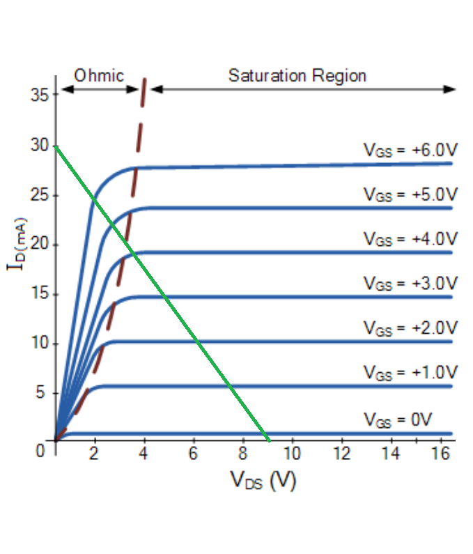
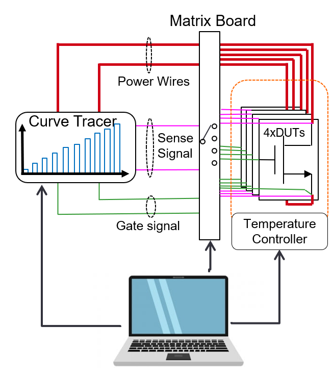
What: Static characterization of commercial GaN HEMTs from major vendors at 50-400K.
How:
- Used commercial curve tracer for static charctierzation : I-V and leakage characterization
- Use of cryocooler based environmental chamber to achieve desired temperatures
- Design of automated setup to cycle temperatures and characterize 4 samples consequently
- Characterization of commercial GaN HEMTs from major vendors at targeted temperatures of 50-400K.
- Positive, negaive and leakage characterization of samples including transfer characteristics.
For our year-long undergraduate capstone project, we designed and optimized a wireless power transfer system for a commercial electric scooter. We successfully demonstrated a working hardware prototype, which was well received by the department.
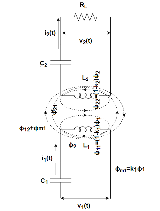
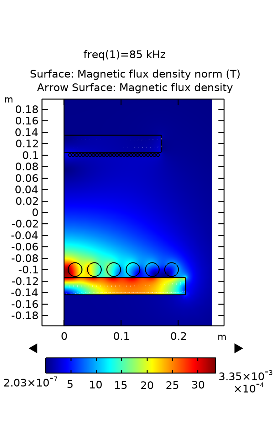
What: Simulation and hardware prototype development of inductive resontant coupling based wireless power transfersystem for electric scooter - transfering power from ground pad to coil at base of the scooter.
How:
- Design and optimization of coil design at given constraints in COMSOL Multiphysics Tool
- Design of half bridge inverter with inductive power transfer using S-S topology
- Design of gate driver circuits using isolated-tranformer topology
- Development of hardware prototype using matrix board and off the shelf parts
- Successful design and demonstration of working prototype on project defence
- Optimized coil design within dimensional constraints and limiting maximum flux density to 80 mT
- Working hardware prototype with power transfered upto 150W achieving maximum power transfer efficiency of 90%
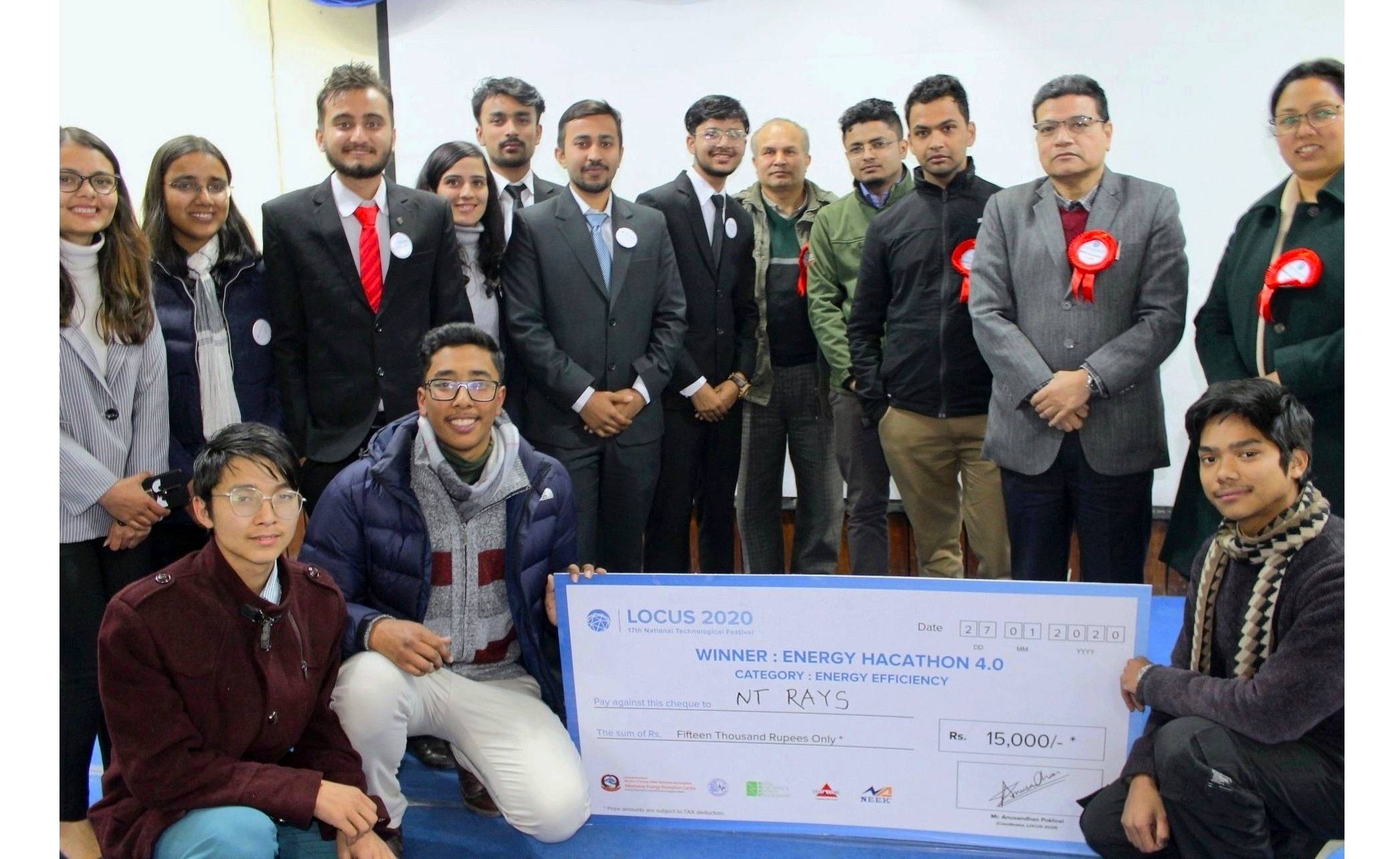
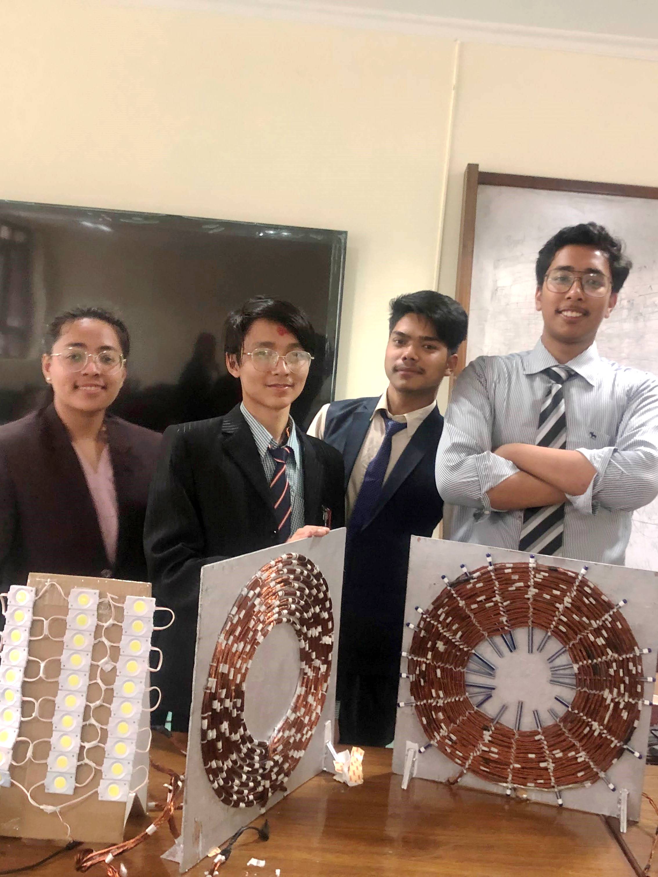
As part of an energy hackathon organized to explore sustainable solutions, we studied the feasibility of replacing traditional LPG-based cooking in the Kathmandu Valley with an induction heater-based approach. Our analysis considered projected energy generation and demand trends over the next five years. To support the case for local adoption, we built a functional induction heater prototype demonstrating the potential for in-country production. Our team won the hackathon in the efficiency category.
Collaborators: Abinash Man Karmacharya, Peter Multiverse (Ganesh Rai), Anjana Shrestha
What: Case study of induction heater cooking to replace LPG cooking in Kathmandu Valley with in-country manufactoring
How:
- Use of official Nepal Electricity Authority (NEA) data for demand and generation of electrical energy
- Local manufactoring of induction heaters for cost effective heaters production
- Comparison and feasibility of the induction heater based solution at peak loading hours
- With clear upward generation trend surpassing electricity consumption demand, the study showed that future generation is capable of providing heater cooking demand
- Comparing cooking cost to LPG cooking revealed about 50% save in energy cost
- Updating grid side stability components and infrastructure revealed the shorter payback period
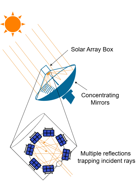
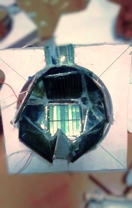
In Himalayan regions, solar panels operate under significantly lower insolation, reducing their power output and overall feasibility. To address this, we designed a system that improves panel efficiency by concentrating solar rays and minimizing reflection losses through effective light trapping.
What: Ferrous black body inspired solar rays concentraing system to improve utility of solar panels
How:
- Large parabolic rays concentraing disc panel to increase solar intensity to panels
- Solar box to trap incident rays to reduce losses in reflection
- Use of mirros to fill in gaps to redirect rays
- 50% increase in solar panel output
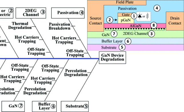
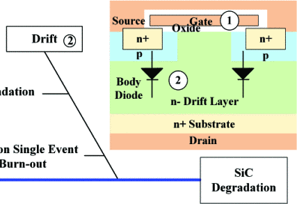
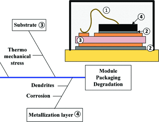
Abstract: The reliability of power electronic (PE) systems is becoming increasingly critical as these technologies are integrated into mission-critical applications. Accurate lifetime prediction for high-failure-rate components, such as power semiconductors and packaging, is essential for ensuring long-term efficient system performance. However, developing high-fidelity lifetime models requires a thorough understanding of underlying physics-of-failure (POF) mechanisms and extensive stress testing, which is often prohibitively costly and time-consuming when conducted individually. This study addresses these challenges by establishing a centralized reliability database, developed through a comprehensive survey of failure mode and effects analysis (FEMA) for the most vulnerable components in PE systems. Lifetime models associated with dominant failure mechanisms are compiled and standardized, including the extraction of key model coefficients, to support consistent and efficient reliability assessments. The resulting database serves as a valuable resource for benchmarking and guiding future research. The focus is placed on wide bandgap (WBG) power semiconductors and module packaging, two of the most failure-prone elements in modern power electronic converters. Additionally, this study identifies existing research gaps and proposes a structured roadmap for advancing the development of a comprehensive reliability database.